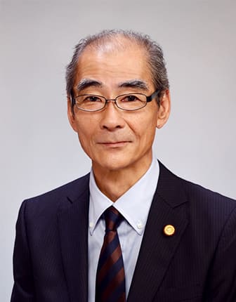
Kenichi KATAYAMA
BIOGRAPHYDeputy Director Kenichi KATAYAMA, after completing graduate work in Physics at Tohoku University, joined the chemical company Showa Denko where he spent 16 years working on the research and development of electronic materials. During this time he also conducted research as a visiting researcher at the Ministry of International Trade and Industry as well as in the Materials Engineering Department of North Carolina State University in the U.S. In 1993 Mr. Katayama then received his Ph. D from Osaka University.
Mr. Katayama passed the patent attorney exam and registered as a patent attorney in 2000 and worked for the JPO and law firms in Tokyo.
He specializes in a wide area of technical fields, including semiconductor devices, display devices, optoelectronics, optics, magnetic recording technology, ceramics, material engineering, and analytical evaluation technology.
As a member of the Japanese Patent Attorney Association, Mr. Katayama is a member of the International Affairs Center. In 2014 he attended the “Symposium of the Topic of the Practice Around Art. 123(2) EPC held by the EPO as a representative for the JPAA. In 2015 he served as the leader of the JPAA’s Europe Visit Group.
He also studied (but did not complete) doctoral work on competition law at the Department of Business Law, Graduate School of Business Sciences, University of Tsukuba.
Mr. Katayama has received high acclaim in both the Individual and Prosecution Department categories every year from the IAM Patent 1000-The World ’s Leading Patent Practitioners, and in 2019 assumed the position of Deputy Director at Sakamoto and Partners.
PRACTICE AREASMr. Katayama is a certified patent attorney who specializes in affairs related to Intellectual Property rights. He has done work in the areas of prosecution, prior art searches, appeals and litigation related to patents, designs and trademarks particularly in the areas of chemistry and electronics (electronics, semiconductor devices, displays, optoelectronics, optical circuits, optics, magnetic recording technology, ceramics, materials engineering, and analysis evaluation technology).
EDUCATIONTokyo University of Science, Department of Physics
Tohoku University, Ph. D in Physics
University of Tsukuba, Department of Business Law, Graduate School of Business Sciences (withdrew as a doctoral candidate)
EXPERIENCEShowa Denko Co., Ltd.
TMI Associates
Tani & Abe, p.c.
Ohno & Partners
PROFESSIONAL ASSOCIATION AND MEMBERSHIPJapan Patent Attorneys Association (JPAA)
ACTIVITIES
| 2002 | Japan Patent Attorneys Association International Activities Committee Member |
|---|---|
| 2003-2004 | Japan Patent Attorneys Association Training Committee Steering Committee |
| 2008 | Industrial Competitiveness Promotion Committee Member |
| 2012- | Present Japan Patent Attorneys Association International Activity Center Member |
| 2013 | JPAA IP Practitioners Seminar in Bangkok, Thailand Lecturer |
| 2013 | Japan Patent Attorneys Association European Visiting Group Member |
| 2014 | “Symposium on the Topic of the Practice Around Art. 123 (2) EPC” Representative for the Japan Patent Attorneys Association |
| 2015 | JPAA IP Practitioners Seminar in Jakarta, Indonesia |
| 2015 | Japan Patent Attorneys Association European Visiting Leader |
| 2017 | JPAA IP Practitioners Seminar in Hanoi, Vietnam Lecturer |
PUBLICATIONS AND PRESENTATIONS◆K. Katayama
"Characterization of Oxygen Precipitates in CZ-Silicon Crystals by Light-Scattering Tomography"
Jpn. J. Appl. Phys. 29 (1990) L198
◆K. Katayama, Y. Kirino and F. Shimura
"Non-contact Characterization for Energy Level Related to Silicon Wafer Surface" in "Defects in Silicon II"
(Eds. W. M. Bullis, U. Goesele and F. Shimura, The Electrochemical Society, Pennington, NJ, 1991) pp.89
◆K. Katayama and F. Shimura
"LM-DLTS Measurements for CZ Silicon Wafers with Different [Oi], [Cs] and Thermal History"
in "Defects in Silicon II"(Eds. W. M. Bullis, U. Goesele and F. Shimura, The Electrochemical Society, Pennington, NJ, 1991) pp.97
◆K. Katayama, Y. Kirino and F. Shimura
"Effects of Ultraviolet Light Irradiation on Non-contact Microwave Lifetime Measurement"
Jpn. J. Appl. Phys. 30B (1991) L1907
◆J. Partanen, T. Tuomi and K. Katayama
"Comparison of Defect Images and Density Between Synchrotron Section Topography and
Infrared Light Scattering Microscopy in Heat Treated Czochralski Silicon Crystals"
J. Electrochem. Soc. 139 (1992) 599
◆K. Katayama and F. Shimura
"Non-contact Defect Characterization for CZ Silicon Crystals with FT-IR, LM-Lifetime, LM-DLTS and Light Scattering Tomography"
in "Diagnostic Techniques for Semiconductor Materials and Devices" (Eds. J. Benton, G. Maracas and P. Rai-Choudhury, The Electrochemical Society, Pennington, NJ, 1992) pp.184
◆K. Katayama and F. Shimura
"Non-contact Characterization for Ultraviolet Light Irradiation Effect on Si-SiO2 Interface"
Jpn. J. Appl. Phys. 8A (1992) L1001
◆A. Buczkowski, K. Katayama, G. A. Rozgonyi and F. Shimura
"Non-contact Mobility Measurement with a Laser/Microwave Photoconductance Technique: Temperature Dependence"
Appl. Phys. Lett. 60 (1992) 1229
◆L. Zhong, A. Buczkowski, K. Katayama and F. Shimura
"Transient Recovery of Minority-Carrier Lifetime in Silicon After Ultraviolet Irradiation"
Appl. Phys. Lett. 61 (1992) 931
◆K. Katayama and F. Shimura
"Noncontact Characterization for Ultraviolet Light Irradiation on Si-SiO2 Interface"
in "Defects Engineering in Semiconductor Growth, Processing and Device Technology"
(Eds. S. Ashok, J. Chevallier, K. Sumino and E. Weber, Materials Research Society, Pittsburgh, 1992)
◆K. Katayama, A. Agawal, Z. J. Radzimski and F. Shimura
"Investigation on Defects in CZ Silicon with High-Sensitive Laser/Microwave Photoconductance Technique"
Jpn. J. Appl. Phys. 32 (1993) 298
◆K. Katayama and F. Shimura
"Noncontact Characterization for Carrier Recombination Center Related to Si-SiO2 Interface"
Jpn. J. Appl. Phys. 32 (1993) L395
LANGUAGEJapanese and Englishsh
HOBBIESGolf

